Abstract:
Transmission electron microscopy provides focused probes of 50 picometers and enables the ability to study low dimensional materials atom by atom. Using advanced direct electron detectors combined with low-dose and low energy electrons, the atomic structure of ultrathin 2D materials can be studied with unprecedented detail. I will show results on the structure of single atom dopants, vacancy defects, dislocations and their dynamics at the atomic scale in 2D layered materials of graphene, hBN, MoS2, WS2, PdSe2, PtSe2 and PbI2. I will then show how using an ultrathin graphene layer as an electron transparent support enables the imaging of small molecules and their self assembly. I will show how the electric field can be mapped around single atoms to show charge densities and nanoscale dipoles. Finally, I will discuss how using in-situ heating holders in TEM enables the clean environment to study vacancy diffusion and migration, revealing how defects aggregate and release strain by various mechanisms.
Biography:
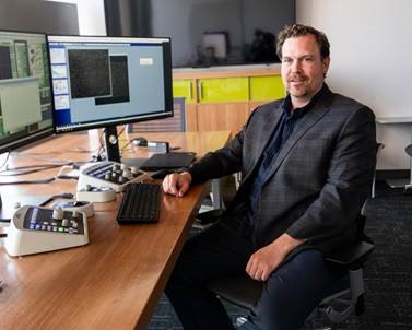
Jamie Warner is the Director of the Texas Materials Institute, and Hayden Head Centennial Professor in the Department of Mechanical Engineering at the University of Texas at Austin. Prior to this, he spent 13 years as Professor of Materials in the Department of Materials at the University of Oxford. His research involves understanding the atomic and nanoscale structure of low-dimensional materials using advanced electron microscopy. In particular, he has pioneered low-voltage transmission electron microscopy to study single atoms and defects in monolayer 2D materials. His work includes advancing in-situ capabilities in TEM, such as heating and electrical biasing, as well as the integration of new direct electron detectors for 4D-STEM and EELS.